Here is the schematic of the board.

The layout of the board.
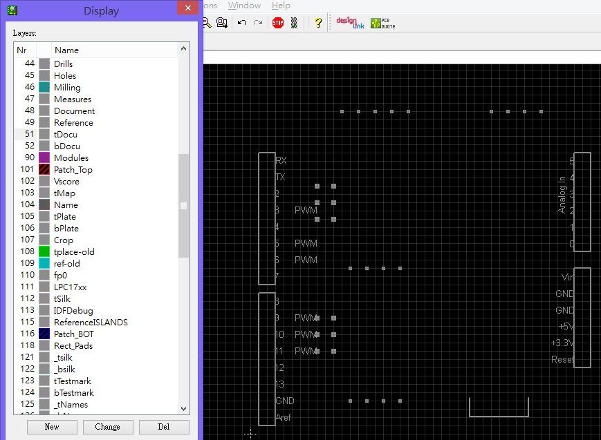
In the Display window to the left, the layers used are highlighted in blue.


The board is a 2-layer board. There are traces on the top and the bottom layers.
Traces on the top layer.

Traces on the bottom layer.

The solder pads are on layer 17.

The via that enables a trace to travel between layers is on layer 18.

The board outlines and circle for holes are on layer 20. This info. will be used by the board manufacturer to cut the board into the desired shape and size.

Layer 21 and Layer 22 are for silkscreen.

The origins of the devices placed on the board are on layer 23 and layer 24.

The names of the devices are on layer 25 and layer 26.

The values of the devices are on layer 27 and layer 28.

The layers that define where soldermask should not be applied are on layer 29 and 30.


Reference:
Using EAGLE: Schematic
https://learn.sparkfun.com/tutorials/using-eagle-schematic
Using EAGLE: Board Layout
https://learn.sparkfun.com/tutorials/using-eagle-board-layout
**Introduction to EAGLE - Understanding layers** <- Very useful!!
http://www.lucidarme.me/?p=2363
No comments:
Post a Comment